Guides / Process
Semiconductor Jigs and Fixtures: Which Part Family, What to Specify, What Fails and Who Makes It
November 21, 2026
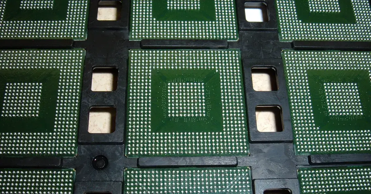
Semiconductor jigs and fixtures are the plates, nests, carriers, pallets and tools that hold a package, a lead frame strip or a board in a known place at one step of assembly or test. Choose the part family from the process step, specify the locating feature tightly and the rest of the part loosely, size every pocket to the worst case and buy the wear parts as spares. This guide is for process engineers, equipment engineers and buyers at assembly and test plants, and it leads to one decision: what to put on the drawing and whom to ask to make it.
You send one RFQ and we quote the finished parts, place the work with a Vietnamese partner shop and follow the run. How we choose shops is on how an order runs.
Last reviewed: October 2026. Figures carry the source they came from; confirm package, tray and handler data against your own customer documents.
- Part families by process step
- Test handler change kits and burn-in fixtures
- Reflow carriers, solder pallets and nozzles
- Lead frame magazines and trim and form tooling
- Die attach, wire bond and advanced packaging tooling
- Assembly, kitting and line parts
- JEDEC trays and custom carriers
- Designing a package nest
- OEM tooling or local tooling
- Why jigs and fixtures fail
- What a jig costs
- Checklist before you send the RFQ
- Send the drawing
Part families by process step
Start from the step, because the step decides what the part has to survive. A die attach heater block lives in heat and a few grams of clamp force. A test handler nest sees a package arriving thousands of times a shift. A wave solder pallet is dipped in molten solder. The table puts the families next to the step that wears them.
| Step | Part families | Where the tolerance lives | Who usually sets the interface |
|---|---|---|---|
| Die attach, wire bond | Heater blocks, window clamps, vacuum chucks, collets | Window position, flat clamping face | Bonder maker |
| Mold and strip handling | Lead frame magazines, strip carriers | Slot pitch, clearance for the warped strip | The plant, from the strip drawing |
| Trim and form | Punches, dies, strippers, form blocks | Punch and die clearance, edge condition | Tool designer |
| Test handler | Change kits, nests, socket plates, trays | Pocket and pitch-related features | Handler maker |
| Burn-in | Stiffener plates, socket lids, guides | Flatness at temperature, hole pattern | Plant and board designer |
| Placement | Pick and place nozzles, die collets | Bore, tip face, shank fit | Placement machine maker |
| Soldering | Reflow carriers, wave solder pallets | Cutout position, pocket depth | Plant process engineer |
| Assembly and line | Assembled fixtures, brackets, rails, guides | Datum scheme, function test | The plant |
Caption: our grouping of the part families covered in this site’s guides. We found no public survey of tolerances by family; typical ranges are in the guide for each family.
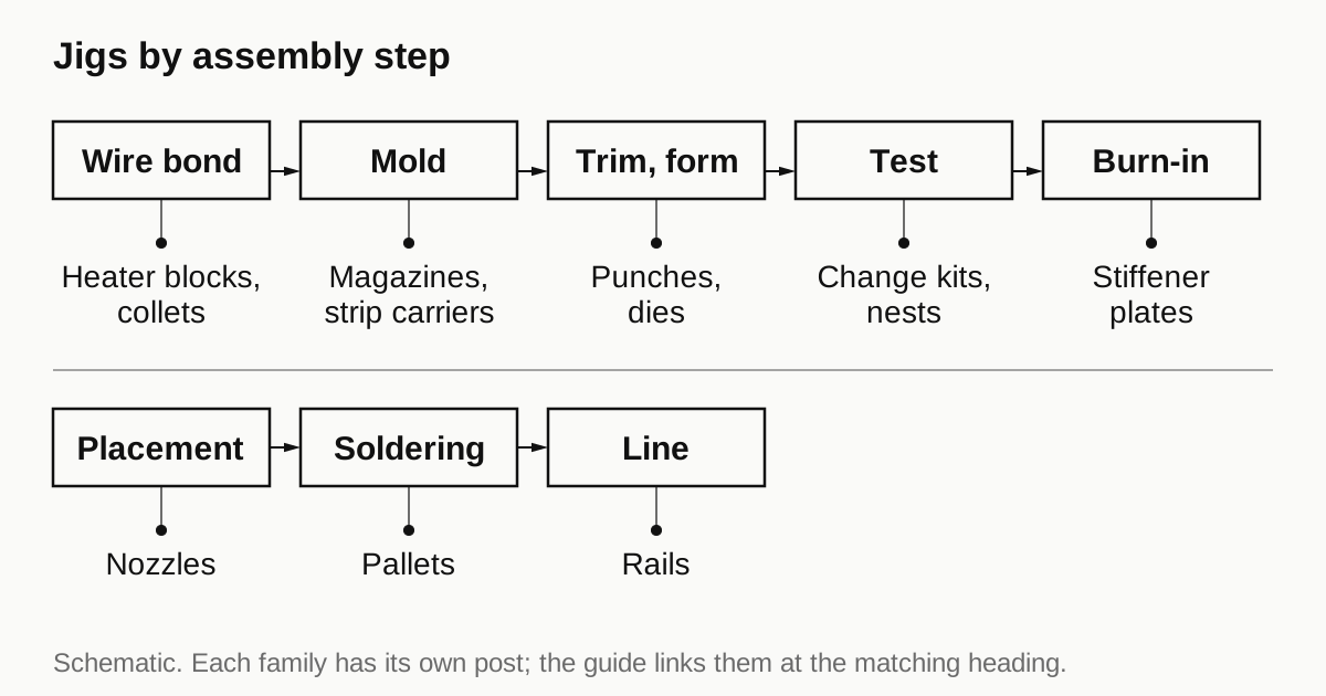
Most of these parts are ordinary machining around a few critical features, so the drawing should say which features those are.
Read more: OSAT assembly and test plants on the industries page
Test handler change kits and burn-in fixtures
A change kit lets one handler run a different package. Advantest describes it as a custom-designed, swappable tool that is part of the handler, and its page lists parts such as match plate, set plate, socket guide, contact chuck and test tray. The machined content is nests, socket and contactor plates and guides. The bought hardware, springs and fasteners is the item people forget until assembly.
The tightest numbers sit on the pocket that locates the package. Package bodies carry tolerances that are large beside fine pitches: a 2005 socket workshop paper called a profile tolerance of ±0.15 mm about the perimeter common for leadless packages, and a Delta Design handler patent says handlers must cope with body tolerances of up to 0.2 mm. A kit is as late as its slowest item, so release the long-lead plastic and hardened parts first and order wear spares with the first kit.
Burn-in boards need a different set: stiffener plates, socket lids, guides and rack hardware. FDA’s inspection guide on screening electronic components gives burn-in temperature as normally 125 °C with an initial burn-in time of 168 hours, so every plastic and every finish must hold at that temperature for days, cycle after cycle. The plate must stay flat in the oven, so stress relieve it before final machining, and fix the board at one point so thermal growth has somewhere to go.
Read more: Test handler change kits and burn-in board and socket fixture parts
Reflow carriers, solder pallets and nozzles
Soldering tooling holds a board flat and shields it from heat. A wave solder pallet supports the board, masks surface-mount parts, opens windows for through-hole pins and takes some of the heat and flux. A reflow carrier holds a thin or irregular board through the oven. Both are made of composite sheet or metal with accurate cutouts, and both are consumed, so a plant with several products holds dozens.
The cutouts carry the tolerance, and the cutout position decides which parts see solder. Ramps and thieves, the shaped cuts that let the wave reach a pin and draw off excess solder, are set by the process engineer, so the drawing or the 3D model must state them. The material rating comes from the sheet maker’s data sheet for the exact grade, because ordinary FR4 is usually a test fixture material and not a pallet material.
Pick and place nozzles and die collets are the opposite case: tiny parts with one critical surface. A vacuum draws the component against the tip, and, to a first approximation at a fixed vacuum, holding force scales with the area of the bore. A bore that is too large draws a small part in and tilts it, and one that is too small drops it under acceleration. The sizing is a calculation plus a trial.
The shank and the spring seat must match the head exactly, so copies come from the maker’s drawing or an unworn part, followed by a trial lot before the batch.
Read more: Reflow carriers and wave solder pallets and pick and place nozzles and collets
Lead frame magazines and trim and form tooling
A lead frame magazine carries strips between assembly steps, and it is where a handling problem turns into a lost lot. The SEMI store listing says SEMI G89 sets the width and length of a lead frame strip for QFP and SOP types, in revision G89-0211, listed as reapproved in 2023, and that it does not cover the unit layout. We did not read the standard text. The lead frame magazine post found no SEMI standard for the magazine itself, so the magazine comes from the equipment maker’s drawing or the plant’s own, and a sample that already runs on the line is the best reference.
Warpage is the number the drawing leaves out. A Philippine plant paper counted 69 crumpled strip cases in six months across four plating machines, 30 on one machine, and its root cause analysis on that machine began with strip warping. Size slots for the worst warped strip you run, and ask for slot pitch measured across the whole magazine.
Trim and form tooling is the other strip-side family. Punches and dies cut the dambar and the leads and bend them to shape, with clearances that the tool designer sets; the trim and form guide on this site puts them at a few micrometers, and we found no public figure. Cutting edges wear and are reground, so the tool is a scheduled spare: ask for the regrind stock, the number of regrinds and the usual shots between regrinds, because a shop that replaces a punch needs the first two to put the right length on it.
Read more: Lead frame magazines and strip carriers and trim and form tooling for OSAT lines
Die attach, wire bond and advanced packaging tooling
As the wire bond post sets out, wire bonding and die attach tooling split into three groups. The bonding tool, a capillary or wedge, is a specialist part. The machine and its head belong to the bonder maker. The work holding, meaning heater blocks, window clamps, top plates and vacuum chucks, is plain precision machining with special requirements, and it is where a machine shop can help. Heater blocks need flatness and thermal stability, window clamps need window position and a flat clamping face, and vacuum chucks need flatness and a leak-tight hole pattern.
Advanced packaging pushes the split further toward the equipment maker. The advanced packaging post, which draws on published papers and trade press, finds that fan-out and hybrid bonding set tighter limits on warpage, particles and placement than older packages, and that the parts that set accuracy, such as carriers, bond heads and process chucks, belong to the equipment makers and wafer suppliers. The jigs around them, such as inspection plates, transfer frames and trays, are ordinary precision work.
The honest answer to a request for a nozzle or chuck at the bond head is often no, or a referral to the maker. A shop that quotes it without the maker’s drawing and qualification is guessing. State in the RFQ whether the part touches a die or a wafer.
Work from a physical reference where you can. The same few parts are reordered for years, wear and are replaced with a sample in hand, which is where a drawing and a first article report earn their cost.
Read more: Wire bond and die attach tooling parts and advanced packaging tooling
Assembly, kitting and line parts
A fixture drawing lists parts, but a fixture in use is an assembly: plates pinned together, bushings pressed in, springs set, hardware torqued and a gauge check that it all holds a position. Between the drawing and the working fixture lie steps that cost real hours, so decide the level of delivery before the order.
| Level | What arrives | Who carries the risk |
|---|---|---|
| Loose parts | Each part checked against its own drawing | Buyer, for how the parts fit together |
| Kit | Parts, hardware and consumables counted, with a bill of materials and an assembly drawing | Shop for completeness, buyer for function |
| Assembled and tested | A built fixture with a record of the checks | Shop, against the stated criteria |
Caption: delivery levels as described in the fixture assembly guide on this site.
If you order assembled fixtures, write the function test into the order: what is checked, with which gauge or master part, and what the pass limit is. Ask for torque and press-fit records where the fit is tight.
Line parts are the other end of the range. The automation parts post sorts them by how easy they are to source locally: brackets, sensor mounts, covers, conveyor rails and simple grippers are easy, while precision shafts and wear parts are narrower. For a plant in Vietnam, the main benefit of a local shop is time: a bracket made nearby can arrive in days, and a line stopped for a missing part costs more than the part.
Turn one-off orders into a spares plan, and protect your drawings with an NDA before they leave the plant.
Read more: Buying assembled fixtures: kitting, torque records and function tests and automation and line hardware for OSAT plants
JEDEC trays and custom carriers
A JEDEC matrix tray is a flat tray of fixed outline that holds packaged chips in rows of pockets. A US patent that cites JEDEC publication 95-1 gives the outline as 322.6 mm by 135.9 mm, and a tray vendor gives the same. Thickness is where sources differ: the vendor lists 6.35 mm and 10.16 mm, and the patent lists 7.62 mm and 12.19 mm. We could not open the JEDEC documents, which are registration-gated, so the thickness is not verified.
The outline is common and the pocket is not. Pockets are cut to the package, and we found no public figure for the pocket tolerance. The tray vendor also says to stack trays only within the same family and model and that bakeable ratings are stamped on the tray, so a custom carrier has to match the outline, the orientation features, the stacking and the bake rating, then add the pocket.
A machined carrier makes sense when no standard tray fits, when the volume is low or when the package is still changing. We found no public tooling cost for a molded tray, so ask for both quotes on the same package drawing. When you write the RFQ, name the tray document and revision your customer holds and state the surface resistance range as a separate line.
Read more: JEDEC matrix trays and custom carrier trays
Need a quote for this part? Get a quote
Designing a package nest
A nest is a pocket that holds a device in a known place for the next step. Size it from the package outline limits, a clearance so the largest package never jams and the wear you accept before the pocket is replaced. Then check that the smallest package, sitting hard against one wall, still lands inside the capture window of the next stage.
The method comes from a 2005 socket workshop paper. The largest pocket equals the largest package plus the clearance plus twice the pocket edge tolerance, and the free play is the pocket size minus the smallest package. In its worked case, a package of 5.9 to 6.1 mm, a clearance of 0.010 mm and an edge tolerance of 0.025 mm per side stack up with the contact errors to a worst-case probe that misses the pad by 0.16 mm. The same logic applies to a handler nest.
An assumed example in the nest post shows it: a 7.00 mm package with a 0.15 mm tolerance in a 7.20 mm pocket has 0.37 mm of free play in total, 0.185 mm each side, before wear and temperature. The post also lists the thermal growth of aluminum, POM and glass epoxy, because a hot or cold test changes the clearance. We found no public standard for lead-in angle, so take it from the maker’s drawing.
Read more: Designing a package nest: pocket size, clearance, lead-in and datum
OEM tooling or local tooling
For most parts that touch the device, the equipment maker’s spare is the first choice. A local copy to the plant’s drawing is workable when the plant owns the drawing and a trial run is allowed. A local design from a worn sample is the option to avoid. For plates, magazines and pallets, whose inputs the plant defines, local tooling is often the first choice.
| Part family | OEM spare | Local copy to the plant’s drawing | Local design from a sample |
|---|---|---|---|
| Handler nest, socket or guide plate | First choice | Workable with a trial | Avoid |
| Nozzle or collet | First choice | Workable with the maker’s interface drawing | Avoid |
| Lead frame magazine | Workable | First choice | Workable with the strip drawing |
| Wave solder pallet | Not applicable | First choice | Workable with the board file |
Caption: our reading of the public record, not a survey. We found no public price comparison between OEM and local parts.
Two public points matter. An Ichor engineer wrote in Silicon Semiconductor in 2018 that a fab cannot simply buy a different spare, because new spare parts typically face a lengthy qualification process, with solutions ranging from days to 12 to 18 months. Warranty terms are a contract matter and we found no public rule that covers every maker, so read your own warranty clause. Settle drawing ownership and the NDA in the order.
Read more: OEM change kits vs locally made tooling
Why jigs and fixtures fail
Fixtures fail on the line in five ways. Strips and devices jam. Contact surfaces wear. Hardware loosens and position drifts. Debris builds up. Static attracts particles. Most trace to a mismatch between what was drawn and what the line sees.
The published cases agree on margin. A pocket or slot sized to the nominal part has no room for the tolerance, and a hand-off without lead-in has no room for a warped strip. The 2004 socket workshop paper adds a design case: when the package is used as a hard stop against the socket floor, mold compound particles and laser mark dust transfer onto the floor over thousands of insertions, and the floor must take the plunger’s shock.
Finish does not settle wear. The Aluminum Anodizers Council guideline says hardness results cannot be used to prove wear resistance, and lists the Taber and ISO 8251 abrasion tests for it. If wear life matters, put the abrasion test and limit on the order. For plastic nests and carriers, an industry article notes that insulators hold charge and attract particles and that grounding cannot remove charge from them, so state a surface resistance range.
Write each limit where the shop can check it and you can verify it, and agree in the purchase order who pays when the line shows a failure the drawing did not cover.
Read more: Why jigs and fixtures fail on the line
What a jig costs
As the cost post sets out, a jig quote is a handful of lines, and most of them are not the metal. Programming and fixturing are paid once per order whatever the quantity, which is why a quantity of one and a quantity of five are closer in total than buyers expect. Machine time follows hole count, pocket depth and the number of flips, not the outline size. Finishing is usually bought outside and adds days as well as cost. Inspection adds hours, and a report on every piece adds them again for every piece.
Four things move the price most: flatness and parallelism, hole position, thread and insert count and the depth of inspection. Tolerance the mounting face, not the whole plate, reference holes to one datum scheme and tighten only the holes that locate something. Order the family of plates together so setup spreads, and order the spare now.
We found no public shop-rate survey or price list for semiconductor jigs, so we give no price here. Compare quotes on the same drawing, with the same inspection depth, the same finish and the same quantity. A comparison of 3D printed, machined and molded jigs for low-volume lines is planned for this guide series and is not published yet.
Read more: What drives the cost of a semiconductor test jig
Checklist before you send the RFQ
The lines that matter differ by family, so the table gives the one line each family most often misses. Use it with the list below.
| Family | The line most orders miss | What goes wrong without it |
|---|---|---|
| Nest or change kit | Package limits and the capture window of the next stage | Jams, or a package that wanders |
| Burn-in parts | Temperature, hours and cycling | A plastic that creeps or an aluminum plate that warps |
| Solder pallet or carrier | Board file, process and material rating | Dry joints, solder on the wrong parts |
| Nozzle or collet | Maker drawing for the shank and a trial lot | A copy that fits and misplaces parts |
| Magazine | Worst-case warped strip and pitch across the whole magazine | A strip that binds or rides up |
| Tray or carrier | Tray document, revision and surface resistance | An outline that fails at the first machine |
| Assembled fixture | The function test and its pass limit | A box of parts that does not hold position |
Caption: our summary of the line each family’s guide flags first.
- The drawing with its revision, and the maker’s drawing for any interface
- Package, strip or board data at both tolerance limits, including the worst warpage you run
- The step and the machine, with the temperature range
- Which features locate the part and carry the tight tolerance
- Material and finish, with the wear test if life matters
- Surface resistance range and cleaning or packing step
- Quantity, spares and the replacement size for wear parts
- Inspection: first article, sampling or full report
- The trial lot, who runs it and the pass limits
- Drawing ownership and the NDA
Send the drawing
Send the list above with the drawing through the RFQ form. We quote the finished parts and place the work with a Vietnamese partner shop, and we reply within 24 business hours with a quote or a plain no. You deal with one contact and get one invoice.
For the material choices behind nests, plates and carriers, see ESD materials and coatings. Confirm package, tray and handler data with your own customer and equipment maker before the order.
Sources
- Advantest, change kit (definition, parts listed for two handler models)
- TopLine, Understanding JEDEC Trays (vendor page: outline, thickness, stacking, bake ratings; directional)
- US 6,082,547, Adapter jig (JEDEC 95-1 tray outline and thickness as quoted)
- BiTS Workshop 2005, session 8: contactor alignment (pocket formula, package tolerance, worked example)
- BiTS Workshop 2004, session 6: leadless package alignment, hard stop wear and debris
- US 10,852,321 B2, Test handler head having reverse funnel design, Delta Design (body tolerance up to 0.2 mm)
- Silicon Semiconductor, M. Firth, the challenges of obsolescence (qualification of replacement parts, 2018)
- Aluminum Anodizers Council, application guideline for hard anodic oxide finishes (abrasion tests, hardness caveat)
- SEMI, G89 specification for leadframe strip size (store listing: scope and revision; text not read)
- FDA, inspection guide: screening electronic components (burn-in temperature and time)
- Allegro MicroSystems Philippines, reduction of crumpled strips, ASEMEP symposium paper (cases and root causes)
- Semiconductor Digest, controlling electrostatic contamination in cleanroom manufacturing (charge on insulators)
Frequently asked questions
What are jigs and fixtures in semiconductor assembly and test?
They are the plates, nests, carriers, pallets and tools that hold a package, a lead frame strip or a board in a known place at one step of assembly or test. Most are plain machined parts with a few critical features, usually the pocket or hole that locates the part. They wear, so most are reordered during the life of a product.
Which part of a handler change kit needs the tightest tolerance?
The pocket that locates the package and the features that set its position to the contactor. Package body tolerances are large beside fine pitches: a 2005 workshop paper called ±0.15 mm common for leadless packages, and a handler patent cites up to 0.2 mm. Tolerance the locating features and leave the rest of the plate ordinary.
Can a local machine shop make parts for an OSAT handler or bonder?
For plates, magazines, pallets and many brackets, yes, when you own the drawing. For parts that touch the device, such as nests, nozzles and collets, the equipment maker's spare is the first choice and a local copy needs the maker's interface drawing and a trial run. A copy from a worn sample is the option to avoid.
What is a JEDEC matrix tray?
A flat plastic tray of fixed outline, quoted in a US patent as 322.6 mm by 135.9 mm, that holds packaged chips in rows of pockets so that machines and people can move them in bulk. The pockets are cut to the package, so a custom carrier can match the outline and differ in the pockets.
Why do fixtures jam or wear out early?
Published cases point at pockets and slots sized for the nominal part, warped strips, hard stops that collect debris and contact surfaces with the wrong finish for sliding duty. An anodizing guideline notes that hardness does not prove wear resistance. Size to the worst case, test the finish and buy spares with the first order.
How do I get a jig quoted from Vietnam?
Send one RFQ with the drawing, the package or strip data, material, finish, quantity and the inspection you want. We reply within 24 business hours with one itemised quote for the finished parts and place the work with a Vietnamese partner shop. You get one contact and one invoice.
Need a quote for this part?
Send the drawing. We quote the finished parts, place the work with a partner shop in Vietnam and reply within 24 business hours.
Get a quoteMore on process
- JEDEC Matrix Trays and Custom Carrier Trays: When Machined Replaces Molded
- Designing a Package Nest: Pocket Size, Clearance, Lead-In and Datum
- Planning Production When Urgent Spares and New Jigs Share the Machines
- Lead Frames Explained: The Metal Skeleton Inside the Package
All guides and the sourcing glossary.