Guides / Process
Advanced Packaging Tooling: What Jigs Fan-Out and Hybrid Bonding Lines Need
November 2, 2026

Fan-out and hybrid bonding put tighter limits on warpage, particles and placement than older packaging, and that shifts the tooling. The parts that set accuracy, such as carriers, bond heads and process chucks, belong to the equipment makers and wafer suppliers. The jigs around them, such as inspection plates, transfer frames and trays, are precision work that a machine shop can quote. This guide separates the two and lists what to put on an RFQ for the second group.
The split below is our reading of the public technical record, not a survey of who makes what. Confirm it with the equipment maker for any part that touches a die or a wafer.
What the two processes do to tooling
Fan-out wafer-level packaging dices the wafer first. The dies are repositioned on a carrier wafer or panel with space kept around each one, the carrier is molded and a redistribution layer is built over the die and the fan-out area. The first fan-out packages were developed by Infineon in the mid-2000s, and high-end versions use lines and spaces narrower than 8 microns.
Hybrid bonding joins copper pads and dielectric directly. Semiconductor Engineering describes it as a glass-to-glass interface with no compliant solder or underfill to absorb a local obstruction, so a single nanosized particle can spoil many units on a wafer. Die-to-wafer bonding picks, aligns and places each die one at a time, which trades wafer-level parallelism for repeated handling.
Three behaviors reach the tooling.
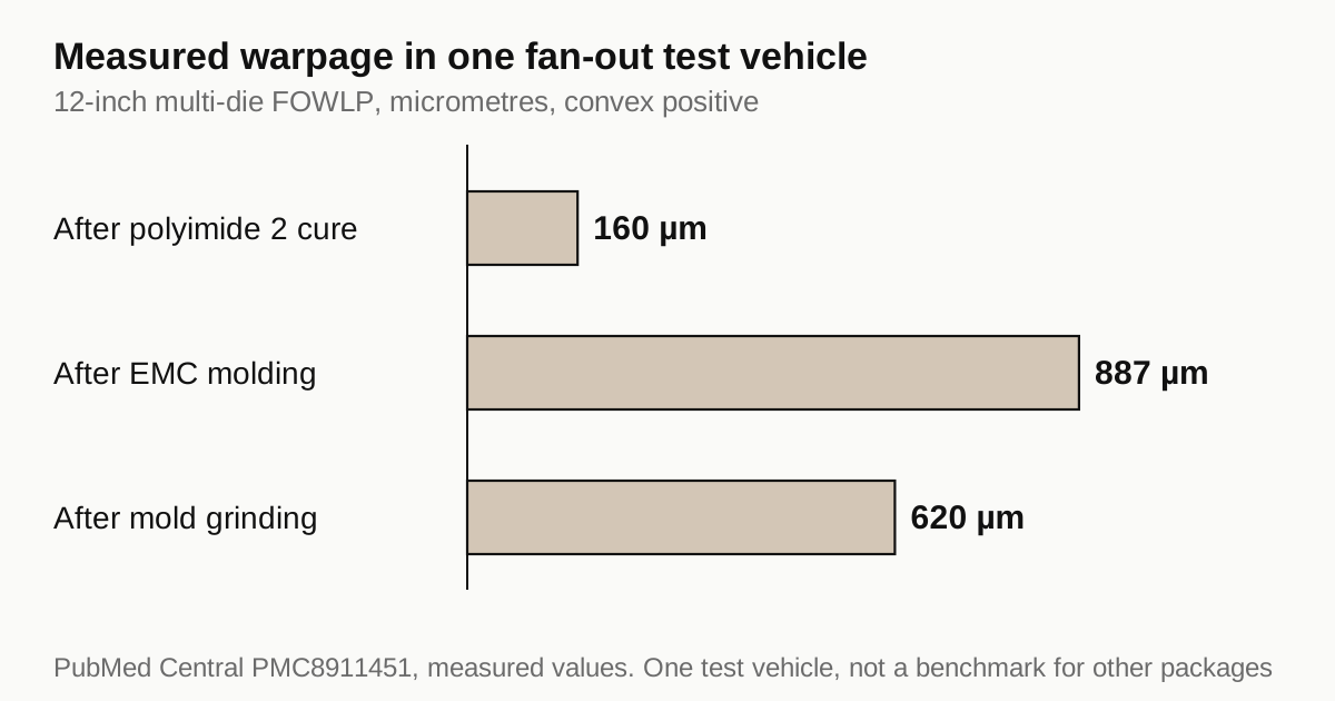
Warpage. The epoxy molding compound has a higher coefficient of thermal expansion than silicon and sits on one side, so the wafer or panel bows after it leaves the carrier. A published finite-element and measurement study of a 12-inch multi-die test vehicle found the molding step the largest contributor, with carrier thickness and thermal expansion the main levers. Measured warpage in that vehicle was 160 micrometres after the second polyimide cure, 887 after molding and 620 after grinding.
Placement error. Pick-and-place adds initial die shift and thermal processing magnifies it. Positional errors of 50 micrometres or more have been reported, against redistribution features as small as 2 micrometres, and larger panels amplify the error. Correction happens at lithography with metrology feed-forward, not in the jig.
Particles and distortion. For hybrid bonding, flatness alone is not enough: wafer bow, local slope and die-level deformation all matter. Contamination can enter at any step between singulation and bonding, including transport and alignment, and queue time is part of the process window.
Why the limits tighten as pitch shrinks
Semiconductor Engineering gives a commercially viable minimum hybrid bonding pitch of about six microns per Amkor, with roadmaps reaching one micron. Its discussion of surface variation makes the tooling link explicit. A local surface distortion that is tolerable at roughly 6 µm can eliminate pad overlap at much smaller pitches. Thickness variation across the carrier stack can shift lithographic focus and leave an offset at the bonding surface that copper-dielectric bonds cannot absorb the way microbumps can.
For a jig, the lesson is about margin, not about a number. A fixture that held a flatness figure on an older package may sit inside a smaller error budget on a new one. Ask the plant’s process engineer for the budget the fixture is allowed to use, and write that figure on the drawing instead of copying the old one.
Who normally owns which tooling
Read the table as a map of risk, not a price list.
| Position in the flow | Tooling | Who normally sets it | Where a jig shop fits |
|---|---|---|---|
| Carrier | Silicon or glass carrier, thickness and expansion matched to the package | Wafer and glass suppliers with the package designer | Not a machined part |
| Warpage adjustment | Heated stage and cold thermal vacuum chuck, contactless handling | Equipment maker | Spares only with the maker’s drawing |
| Bond head | Nozzle, pick tool, bond chuck | Bonder maker | Only against the maker’s qualified drawing |
| Between tools | Cassettes, film frames, trays, shipping boxes | Standards and tool makers | Custom trays and transfer frames for a plant’s own formats |
| Metrology | Flatness plates, reference blocks, inspection fixtures | The plant | Standard precision jig work |
| Line support | Holders for test wafers, carts, bench fixtures | The plant | Standard jig work |
Two points from the sources explain why the first three rows stay with the equipment maker. A published warpage-adjust study found the best result with the wafer held at 200 °C and handled without contact, using an air cushion, before it moved to a cold vacuum chuck. And Intel’s hybrid bonding work found that bonder nozzle geometry changed the directional distortion pattern. Those are tool-design parameters, set and qualified together with the process.
Need a quote for this part? Get a quote
What to put on an RFQ for the jigs around the process
If the part is a fixture, a plate or a frame near the line, write down what the line will do to it.
- Flatness and datums. A flatness figure with its datum scheme and measurement method. Flatness and parallelism on plates covers how to write it.
- Material and thermal behaviour. The material and its coefficient of thermal expansion if a mismatch with silicon or glass matters. State the highest temperature the part will see. If a stress relief or bake step is allowed, say so.
- Contact rules. Which faces may touch a wafer or die, edge-only contact if required, and the finish on those faces. Wafer handling end effector parts covers contact surfaces.
- Cleanliness. The cleanliness class and the cleaning and packaging steps expected. Cleanroom machining requirements shows what each step costs.
- Static control. The surface resistance range if the part touches a die. See ESD materials and coatings.
- Inspection evidence. The first article report and the measurement uncertainty you accept, per first article inspection reports.
Ask the shop to state in writing what it can and cannot measure. A flatness requirement tighter than the shop’s CMM can resolve is a requirement it cannot check.
When the honest answer is no
Some requests belong with the equipment maker. A nozzle or chuck that sets die placement, a carrier that sets warpage or a surface that bonds directly to a die cannot be quoted from a drawing alone. If your part sits in that group, a local shop that quotes it without the maker’s qualification is guessing. We say so rather than quote it. How we decide is on how an order runs.
For the plant side of the picture, Vietnam’s semiconductor buildout lists the packaging sites that are expanding, and automation parts for OSAT plants covers the handling hardware local shops already make.
For the jigs around an advanced packaging line in context, see our guide to semiconductor jigs and fixtures.
If you have a fixture or a transfer frame for an advanced packaging line, send the RFQ and say whether the part touches a die or a wafer. We come back within 24 business hours with a quote or a plain no.
Sources
- Wikipedia, Fan-out wafer-level packaging (process flow, line and space, history)
- Investigation of Warpage for Multi-Die Fan-Out Wafer-Level Packaging Process, PubMed Central open-access article (carrier role, EMC molding, measured warpage)
- 3D InCites, controlling warpage and placement error for FOWLP (die shift, thermal warpage adjustment, contactless handling)
- Semiconductor Engineering, can fine-pitch hybrid bonding go high volume (particles, distortion, die handling, nozzle geometry, six micron pitch)
Frequently asked questions
What tooling does a fan-out packaging line need?
Fan-out dices the wafer first and repositions the dies on a carrier wafer or panel with space around each die. The line then needs carriers, molding and grinding fixtures, thermal chucks, contactless handling and inspection fixtures. Most of the process tooling comes from the equipment maker. The fixtures around it are where a jig shop can help.
Why does warpage drive the tooling design?
The epoxy molding compound has a higher thermal expansion than silicon and sits on one side, so the wafer or panel bows. In one published 12-inch test vehicle the measured warpage was 887 micrometres after molding and 620 after grinding. Carrier thickness and thermal expansion are the main levers that engineers use to control it.
Can a machine shop in Vietnam make hybrid bonding tooling?
The parts that touch the die at the bonder, such as nozzles and chucks, are set by the equipment maker, and a general jig shop should not quote them without that maker's drawing and qualification. Fixtures around the process, such as inspection plates, trays and transfer frames, are ordinary precision work. Say which of the two your part is.
How fine is commercial hybrid bonding today?
Amkor, quoted by Semiconductor Engineering, puts the commercially viable minimum pitch at about six microns, with roadmaps reaching one micron. At that scale the margin for particles, surface variation, distortion and placement error is much smaller than in earlier packaging, which is why cleanliness and flatness requirements on the tooling tighten.
Need a quote for this part?
Send the drawing. We quote the finished parts, place the work with a partner shop in Vietnam and reply within 24 business hours.
Get a quoteMore on process
- JEDEC Matrix Trays and Custom Carrier Trays: When Machined Replaces Molded
- Designing a Package Nest: Pocket Size, Clearance, Lead-In and Datum
- Planning Production When Urgent Spares and New Jigs Share the Machines
- Semiconductor Jigs and Fixtures: Which Part Family, What to Specify, What Fails and Who Makes It
All guides and the sourcing glossary.